您希望搜索哪方面的内容?
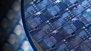
自动化晶圆上测量
半导体器件的准确 DC/CV 和 RF 统计建模需要从不同晶圆在不同温度下收集大量测量数据。
Keysight 为器件建模工程师提供自动化的交钥匙解决方案,以实现更高效的晶圆上测量。该解决方案包括以下功能。
- 超过 50 个交钥匙测量驱动程序,完全针对速度进行了优化
- 全面支持行业标准探测器,例如 Form Factor、MPI、Accretech、TEL 等
- 集成晶圆图支持
- 广泛的测量算法库
- Python/PEL 编程环境可实现自定义测量、后处理算法和通过/失败条件

Accurate, automated on-wafer measurements
On-wafer measurement automation is critical to achieving the throughput and accuracy you need in your production and R&D environments.
Keysight and FormFactor provide all critical building blocks for wafer-level device characterization.
Form Factor’s wafer-level probe station, probes, and calibration tools combined with Keysight’s test instrumentation and measurement and analysis software enable engineers to perform on-wafer DC parametric, IV & CV curves, and calibrated S-parameter measurements on devices at frequencies up to 120 GHz.
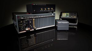
Measure Semiconductor's flicker(1/f) noise with wafer mapping
Keysight provides a turnkey solution to measure flicker (1/f) noise and random telegraph noise (RTN). Keysight's Advanced Low-Frequency Noise Analyzer (A-LFNA) enables a closer look at noise in components, individual devices, and integrated circuits, both packaged and at the water level. Thanks to seamless integration with WaferPro Express software, modeling engineers can program and sequence high-speed DC, capacitance, and RF measurements, while automating wafer prober control.
Find the Product That's Right for You


Featured Resources for 晶圆上测量


Want help or have questions?